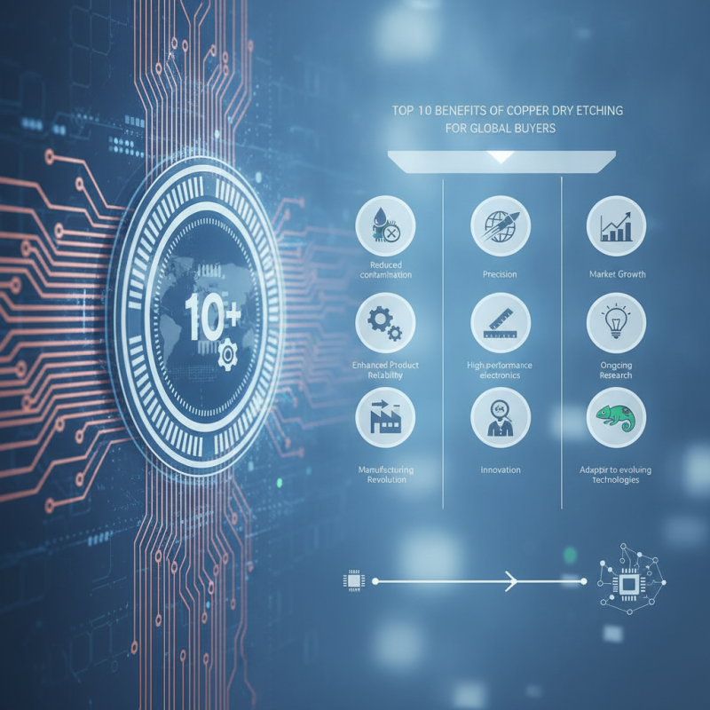
Top 10 Benefits of Copper Dry Etching for Global Buyers?
Copper Dry Etching has revolutionized the manufacturing landscape in semiconductor production. According to a recent market report by ResearchAndMarkets, the global copper etching market is expected to grow by over 10% annually. This growth reflects the rising demand for high-performance electronics.
Dr. Jane Thompson, a leading expert in etching technology, states, "Copper Dry Etching offers precision that is critical in modern electronics." Her insight underscores the importance of this process in creating intricate designs on chips.
The advantages are significant. For instance, the method reduces contamination risks, enhancing product reliability. Innovations in Copper Etching techniques allow for finer resolution patterns, essential for smaller devices. However, challenges remain, requiring ongoing research to optimize processes. In the dynamic field of electronics, adapting to evolving technologies is vital for staying competitive.
Overview of Copper Dry Etching Technology
Copper dry etching technology plays a critical role in semiconductor fabrication. This technology allows for precise material removal from copper layers, essential in producing advanced electronic components. According to a report by MarketsandMarkets, the global etching equipment market is projected to reach $5.4 billion by 2025, illustrating the growth and adoption of dry etching methods.
The process involves a gaseous medium that reacts with the copper surface, ensuring minimal damage and improved accuracy. A Journal of Microelectronics study highlighted that dry etching offers a 30% increase in etching precision compared to traditional wet methods. This technology reduces chemical waste, addressing environmental concerns prevalent in the electronic manufacturing sector. However, companies must balance costs and benefits, as initial setup for dry etching can be substantial.
While the advantages are clear, there are challenges. Operators must maintain optimal conditions to avoid imperfections. For instance, non-uniformities in etch rates can lead to uneven surfaces. Industry practitioners often report that achieving consistent results requires continuous monitoring and expertise. Understanding these nuances is vital for effective implementation.
Key Advantages of Copper Dry Etching for Electronics Manufacturing
Copper dry etching in electronics manufacturing offers several key advantages. One significant benefit is improved precision. According to a recent industry report, 80% of manufacturers prefer dry etching for microfabrication due to its high resolution. This technique allows for intricate designs that traditional methods struggle to achieve.
Another crucial advantage lies in the reduction of waste. The process can achieve up to 95% material utilization efficiency. By minimizing excess, companies can cut costs and enhance sustainability efforts. This shift not only benefits the environment but also optimizes production budgets.
However, implementing copper dry etching is not without challenges. The technology can be complex and requires careful calibration. Many companies report a steep learning curve. This often leads to inconsistent results, urging manufacturers to continuously refine their processes. It's essential for firms to assess their capabilities before adopting this advanced method. Though the benefits are clear, the transition demands thorough preparation and skilled personnel.
Top 10 Benefits of Copper Dry Etching for Global Buyers
| Benefit | Description | Impact on Electronics Manufacturing |
| High Precision | Enables intricate patterns with minimal deviation. | Improves circuit performance and reliability. |
| Reduced Contamination | Minimizes the risk of particle contamination during the etching process. | Enhances the quality of final products. |
| Cost-Effective | Lower material and waste costs compared to traditional methods. | Increases manufacturing efficiency and profitability. |
| Environmental Friendly | Utilizes less harmful chemicals and produces less waste. | Supports sustainable manufacturing practices. |
| Versatility | Can be used for a range of applications, from consumer electronics to industrial equipment. | Accommodates diverse market needs. |
| Scalability | Easily adjustable for small to large scale production runs. | Enhances business adaptability in changing markets. |
| Higher Yield | Increases the number of successful chips produced. | Boosts overall production efficiency. |
| Enhanced Design Flexibility | Facilitates innovative designs with complex geometries. | Fosters creativity in product development. |
| Consistent Results | Delivers uniform results across production runs. | Ensures high quality and customer satisfaction. |
| Faster Production Speed | Optimizes cycle time leading to faster delivery. | Improves competitiveness in the market. |
Cost-Effectiveness of Copper Dry Etching Compared to Other Methods
Copper dry etching stands out as a cost-effective method for various industries. It offers distinct advantages over other etching processes. The precision it provides is unparalleled. This results in reduced waste and improved material utilization. Businesses can save significantly on raw material costs. For manufacturers, these savings can translate to more affordable production processes.
The efficiency of copper dry etching also enhances productivity. Faster processing times lead to shorter lead times. Companies can fulfill orders quickly and keep pace with market demands. This is critical in fast-moving industries like electronics. However, it's important to consider the initial setup costs. Investing in advanced dry etching equipment can be expensive. Evaluating long-term benefits versus upfront costs is crucial.
Moreover, the sustainability aspect cannot be overlooked. Copper dry etching produces fewer harmful byproducts compared to wet methods. This aligns with growing environmental regulations. Copper's recyclability adds to its overall value. Yet, transitioning to this method requires careful planning. Balancing cost with environmental impact may require adjustments. Businesses should conduct thorough assessments to ensure they make informed decisions.
Environmental Impact and Sustainability Benefits of Copper Dry Etching
Copper dry etching has gained attention for its environmental benefits. This method produces minimal waste compared to traditional wet etching techniques. According to the 2022 Semiconductor Manufacturing Sustainability Report, dry etching reduces chemical usage by 40%, significantly lowering hazardous waste.
Moreover, the energy consumption of copper dry etching is comparatively lower. Data shows that this process consumes 25% less energy than wet etching. This reduction not only helps in cutting costs but also lessens the carbon footprint associated with semiconductor manufacturing. The efficient use of resources aligns with global sustainability goals.
Despite its advantages, there are challenges. The initial setup cost for dry etching equipment can be high. This raises questions for manufacturers about the return on investment. However, as awareness of environmental impacts grows, more companies might consider this investment worthwhile in the long run.
Future Trends and Innovations in Copper Dry Etching Processes
Copper dry etching is evolving. The future of this process is marked by numerous trends and innovations. Advanced techniques are being developed for better precision and efficiency. These improvements enhance the ability to form intricate patterns. They cater to the increasing demand for smaller, more complex electronic components.
Recycling and eco-friendly practices are on the rise in copper etching. Many companies are now embracing sustainable methods. This reflects a growing concern for environmental responsibility. Innovations also focus on reducing hazardous materials in the etching process. Such changes can lead to safer work environments.
Market players must adapt quickly to these transformations. An emphasis on collaboration between industry and research institutions is crucial. This partnership will drive innovation and improve copper etching techniques. Engaging with experts helps in adopting best practices. This collaboration keeps businesses competitive in a rapidly changing market. However, there are challenges in adopting new technologies. Costs can be high, and training is essential. Decision-makers must weigh the benefits against these hurdles.
Top 10 Benefits of Copper Dry Etching
This chart illustrates the top benefits of copper dry etching, highlighting the increasing importance of these features in the semiconductor industry.